Simulation and verification results
Link budget (requirement R2)
f-3dB              = 138.2 MHz   (R1 needs >= 50 MHz: PASS)
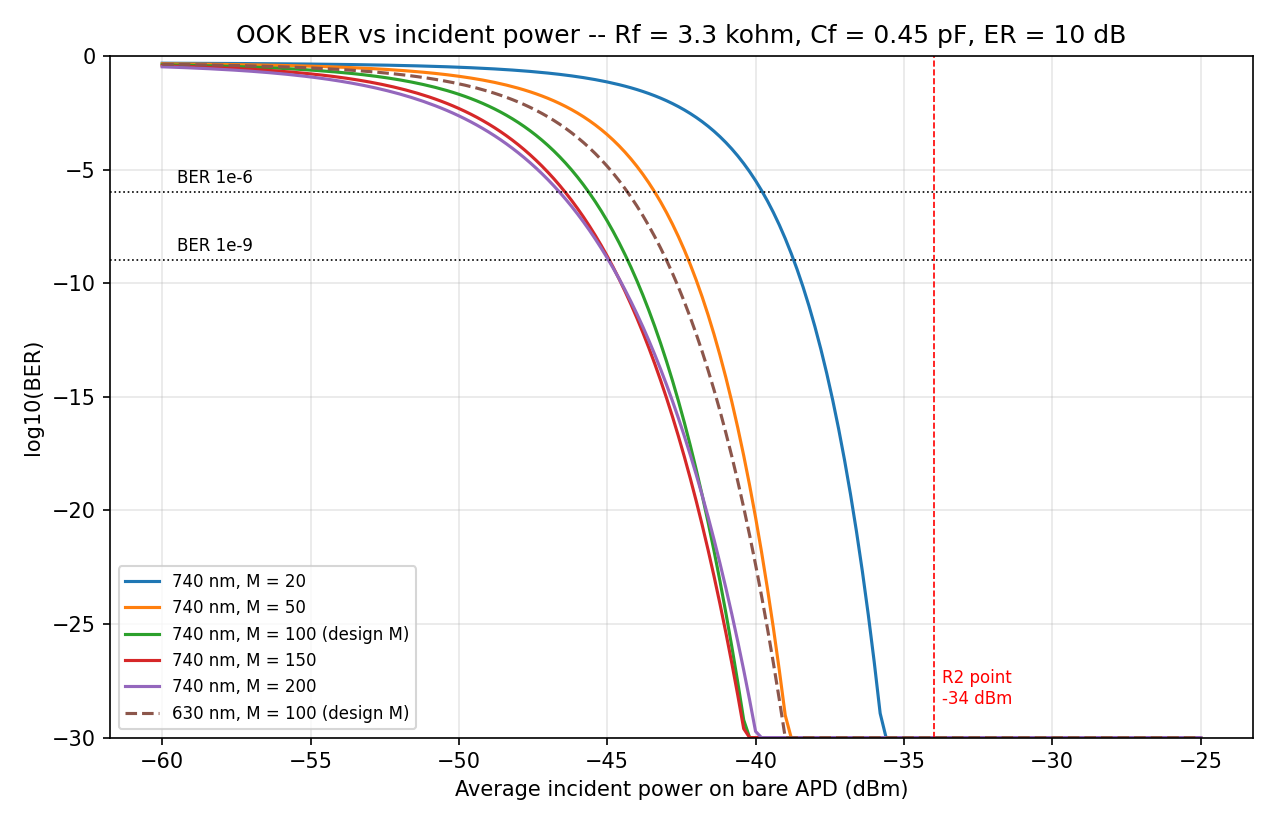
Best sensitivity in sweep: -46.60 dBm at M = 200 (sweep edge region; sensitivity is very
  best sensitivity (-45.62 dBm vs best -46.60 dBm).  Higher M buys <1 dB while moving
3) SENSITIVITY AT THE DESIGN POINT
Chosen design: Rf = 3300 ohm, Cf = 0.45 pF, M = 100, f-3dB = 138.2 MHz
  Margin vs R2: 11.6 dB (sensitivity is that far below the -34 dBm requirement).
  post gain x1: sensitivity = -45.62 dBm (delta vs x1 = +0.000 dB)
  post gain x5: sensitivity = -45.66 dBm (delta vs x1 = -0.046 dB)
  the x5 stage is comparator overdrive: at sensitivity the
     Rf  Cf(pF)  f-3dB(MHz)  Mopt  sens@1e-6(dBm)  Q@-34dBm  verdict
for margin this application does not need (11+ dB already).
certain, not marginal.  That is normal for a receiver with
~12 dB of sensitivity margin below -34 dBm and a 3.3k TIA on
pk-pk -- marginally over 2 ns.  That number rests entirely on
  worst-case sensitivity loss of 0.118 dB, vs a 1-sigma noise fraction
  of 3.6 % at the R2 point and an R2 margin of 11.6 dB.  Ripple-induced AM is well below
  Same sensitivity coefficient, for temperature: at fixed bias
HV RIPPLE VERDICT: PASS (at design M, with temp compensation fitted)
  BARE: A_eff = 0.196 mm^2 -> on-axis range to sensitivity = 19 cm.
        i.e. 8.4 dB BELOW sensitivity: bare mode does not cover a
        range to sensitivity = 2.84 m.
  sensitivity (1/d^2 only; emitter off-axis falloff not modelled).
Chosen design: Rf = 3300 ohm, Cf = 0.45 pF (total, incl. parasitics), M = 100, f-3dB = 138.2 MHz
R1 bandwidth: f-3dB 138.2 MHz >= 50 MHz -- PASS
R2 VERDICT: PASS (locked Rf = 3.3 kohm design passes as originally specified)
TIA ngspice
f-3dB = 153.1 MHz
peaking = 0.00 dB
integrated output noise = 0.567 mV rms (link budget 0.569)
PASS  f-3dB >= 50 MHz (R1)
PASS  peaking < 3 dB
PASS  step settles to 5% within 1 UI (20 ns)
PASS  noise within 3 dB of link budget 0.569 mV
VERDICT: PASS
HV flyback
switching: Vout=408 V open-loop, APD ripple=2.89 mVpp
PASS  switching Vout in 300..600 V band at design Ipk (open-loop power delivery class)
PASS  APD-node ripple < 20 mVpp (R9)
PASS  averaged loop: 150 V pre-step within 5%
PASS  averaged loop: settles within 2% of 420 V
PASS  averaged loop: overshoot < 5%
VERDICT: PASS
Digital simulation
PASS: (a) zero-noise codec, 1e6 bits
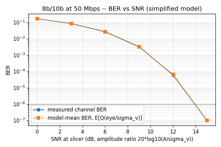
PASS: (b) BER monotonic non-increasing with SNR
PASS: (c) PER sim vs analytic within 4-sigma bound
PASS: (d) BER < 1e-6 at Q=6 SNR over 1e6 bits
PASS: digital_sim -- all checks passed
Schematic netlist verification
netlist check: 630 connected pins, 213 nets, 530 expected connections
PASS: netlist matches circuit.py exactly; structural checks pass
Link budget — BER vs incident power
TIA AC response (ngspice)
TIA AC response render not generated — run scripts/make_fab.sh.
Digital simulation