Pass 112
2026-11-05 10:48 PST (2026-11-05T18:48:09Z UTC) · commit 6df00a1 (6df00a118777ace8727ace42f44bf9bd1b630a9c)
ADOPTED
U4 north gate re-woven; +3V3D_CDR haul REFUSED in all topologies (named residual, full record in hw/fix_gate.py + hw/fix_gate2.py docstrings). Ripped the clock pair’s woven escapes + REFCLK’s two junction vias; heal then connected +3V3D_CDR through the gate (via 54.38,-14.38 + B west run) but that route re-sealed both clock stubs (via-disc tiling, verified site-by-site). Reversed the order: ripped heal’s +3V3D_CDR gate route (7 items), hand-laid REFCLKN (F north + flat into its tail (55.5,-14.5)) and REFCLK (F north at x=53.75, swerve over THRADJ’s via, B bridge over CDR_LOL, In2 drop onto its own tail at (57.35,-13.65)) – both clocks CONNECTED on the audit. heal +3V3D_CDR then refused on the clock-placed field (its optimum is the ripped route), and ~15 hand channel forms were shape-refused: the gate’s F/In2/B capacity fits only 2 of the 3 nets in every topology tried (In1 is an unused plane layer board-wide – 0 tracks – and stays unused). DELTAS vs pass 111: nets 31->31, violations 87->87, unconnected list and clearance census BYTE-IDENTICAL – topology change only: heal’s blocking route is off the board and the clocks hold the new routes, which is the prerequisite field for the next +3V3D_CDR mechanism (east-column re-lay of CF1’s B staircase + CDR_LOL’s escape). +3V3D_CDR stays split: stub (54.75,-15.45) vs main group.
| Nets fully routed | not recorded |
| Pins failed | not recorded |
| Clearance violations | 87 |
| Unconnected nets | 31 |
| Audit verdict | FAIL |
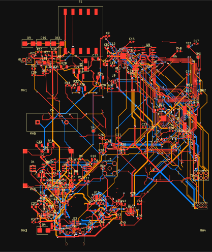
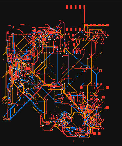
Routes — all copper layers and each layer
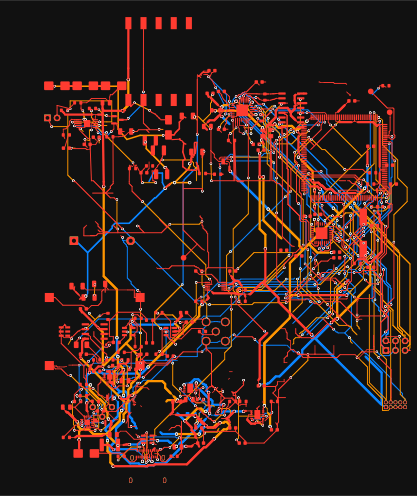
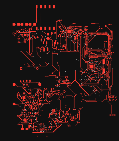
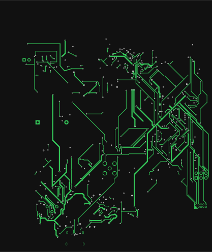
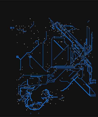
F.Cu In1.Cu In2.Cu B.Cu
Top
Bottom
← Pass 111 · all passes · Pass 113 →