Pass 149
2026-11-06 01:59 PST (2026-11-06T09:59:03Z UTC) · commit fa5c56b (fa5c56be261e09d3ecf641b78a1b2379b8a72cd1)
ADOPTED
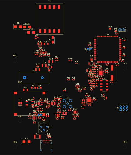
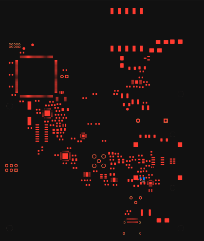
WHOLE-BOARD RE-PLACEMENT (user order 2026-11-06: placement itself was the defect). Force-directed placement over all 139 movable parts: connection springs (per-net pad star) + hard courtyard separation + simulated annealing with same-padcount swaps; anchored: mounting holes, edge connectors J1/J2, shield can SH1 with the APD/TIA under it, alt-APD D2, test header J3; HV creepage slot and board bounds hard constraints throughout. Clusters now sit on their connections: ADN2813 U4 and capture U5 beside J2 on the y=43 latitude; DAC U8 beside the processor; +3V3D regulator U11 moved from the NW corner to its east-side loads; SWD header J4 beside U6 (and U6’s east-edge satellite column – VCAP1/2, LEDs – placed against its pads at x=95.75); interlock J5 in the processor-to-converter corridor at (48,-20). Locality census (scratch/locality.py, same method both boards), exp177 -> exp179: TOTAL pad star 6142 -> 3680 mm (-40%); +3V3D 1367 -> 615 (span 122.0 -> 58.4), +5V 818 -> 585, +3V3A 291 -> 162, APD_K 195 -> 105, +VA 141 -> 82, PG_3V3 141 -> 57, CDR_CLKP/DATP ~110 -> ~43 each; worst parts by mean partner distance: J2 53.2 -> 19.1, J5 46.7 -> 20.3, C9 41.1 -> 15.3, J4 38.6 -> below 13, U8 26.4 -> 14.9, U6 22.9 -> 13.9. Remaining far parts are geometric floors, named: D3 (USB PHY pair to U7, USB cluster kept), T1 (transformer pad spread), J5 (series midpoint between processor and converter), D8 (emitter at the detector). Courtyard: 0 gated pairs (full check_pcb audit); SH1 fallback pairs 21 (the standing blind spot; SH1 did not move). One FD casualty found by DRC and fixed before commit: C41 had drifted onto SH1’s GND pad (SH1 has no drawn courtyard, so the placer could not see it) – moved clear to (31,50.5). Copper: STRIPPED (0 tracks, 0 vias verified on the saved file) – the re-placement orphaned effectively all routing; the board is re-routed from here as the main job. KiCad DRC on the bare board: 154 violations, all non-copper except 4 (J1 footprint-intrinsic edge items: NPTH vs own A12 pad, shield pads vs south edge) + 1 solder-mask bridge (C41 -VA pad vs GND pour); silk_overlap/silk_over_copper 148 (designator text collisions from the moves, tail class); shorting 0; unconnected 303 (every net, by construction). The exp177/178 line remains in git history; this board is the board now.
| Nets fully routed | not recorded |
| Pins failed | not recorded |
| Clearance violations | 15 |
| Unconnected nets | 120 |
| Audit verdict | FAIL |
Routes — all copper layers and each layer
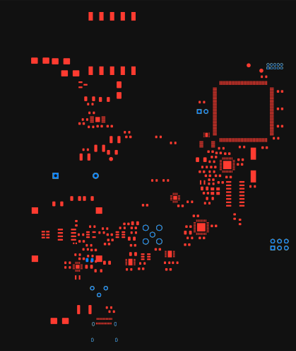

F.Cu In1.Cu In2.Cu B.Cu
Top
Bottom
← Pass 148 · all passes · Pass 150 →