Pass 181
2026-11-06 15:27 PST (2026-11-06T23:27:14Z UTC) · commit 99fc2b5 (99fc2b58b2cae7a6685f5a537c6b1b6ae484b5aa)
ADOPTED
pass 181: I2C_SDA connected (U4.21 end) — heal (astar6) threaded the SE staircase bundle in 31s with 5 vias where hand analysis had proven the only F channel sealed (0.575mm between C46.2/X2.1 pads vs 0.6 needed) and costed a 6-via manual weave across REFCLK/DM_PHY/DP_PHY/+5V/BIST_DRV bands; DRC delta zero. Side experiment t_z1 (evidence, not banked): an I2C_SDA track laid on In1 grazing the RBIAS through-via at (69.625,20.625) by 0.025mm came back from save/reload renamed RBIAS — the save-rename mechanism is CONTACT with any foreign copper sharing a layer (track/via/pad/fill), not the fill alone; clearance-legal tracks are safe, and In1 (solid GND plane) is unusable for signals. DRC: unconnected 22->21, violations 154->154 identical class table, clearance/shorting/dangling 0
| Nets fully routed | not recorded |
| Pins failed | not recorded |
| Clearance violations | 108 |
| Unconnected nets | 18 |
| Audit verdict | FAIL |
Routes — all copper layers and each layer
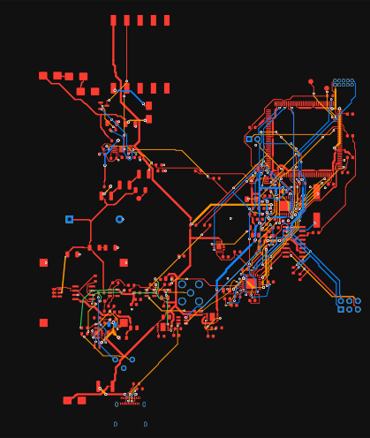
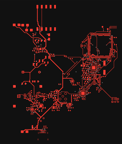
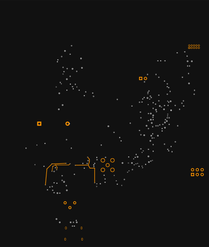
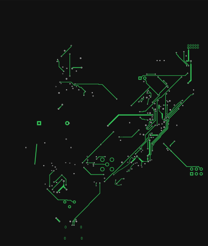
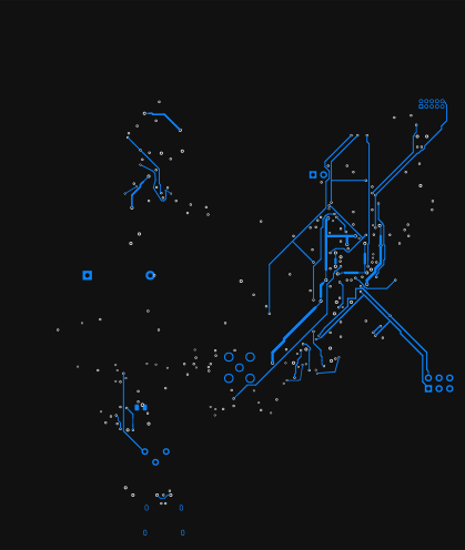
F.Cu In1.Cu In2.Cu B.Cu
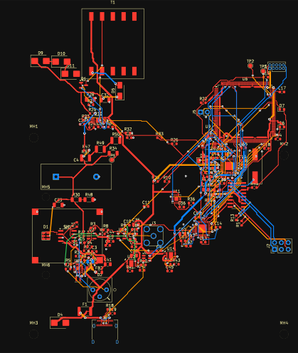
Top
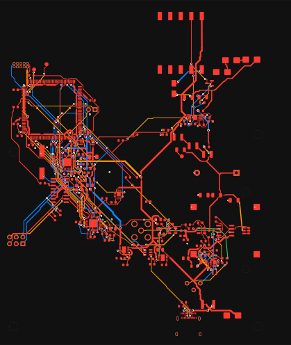
Bottom
← Pass 180 · all passes · Pass 182 →